AN54LV-15 — nRF54L15 MCU module (selected second source, B2)¶
Raytac AN54LV-15 — selected second-source module for the nRF54 platform (decision 2026-08-20 — ECN-19). Introduced on the new article family 232220–232224 / 230240 / 230242 (A1) — see ECN-23 and Article Numbering.
Why this module: nRF54L15 WLCSP/CSP silicon → +8 dBm TX and all 32 GPIOs incl. P1.15 = full functional parity with PAN B611-1 (zero firmware delta — no LPD workaround, no TX-cap differentiation), complete fresh certifications including ISED (Canada), integrated antenna, and a smaller footprint than PAN611.
| Manufacturer | Raytac Corp (Taiwan) |
| Ordering code | AN54LV-15 (chip antenna; regulatory model "AN54LV") |
| Sibling variants | AN54LV-P15 (PCB trace antenna) · AN54LV-U15 (u.FL) · AN54LV-K15 (ANT pad — own-antenna track) |
| SoC | Nordic nRF54L15 WLCSP (stated in datasheet) — 1.5 MB NVM / 256 KB RAM |
| Dimensions | 8.4 × 6.4 × 1.5 mm (55 bottom LGA pads; pads 46–55 = GND under antenna) |
| Antenna | Integrated ceramic chip antenna (PIFA), peak gain +0.57 dBi, efficiency 32–40 % (SGS-measured, DS §7) |
| Crystals | 32 MHz onboard; 32.768 kHz NOT onboard — external crystal on XL1/XL2 required (see Host BOM delta) |
| TX / RX | −? …+8 dBm (CSP) / −96 dBm class @ 1 Mbps |
| Supply | VDD_NRF (pad 20); DC/DC mode requires external L1 4.7 µH between DCC (pad 28) and DECD (pad 30), else LDO mode |
| Temp range | −40…+105 °C |
| Certifications | See table below — incl. ISED 8017A-AN54LV |
| Sourcing | DigiKey Marketplace $4.30 @1 / direct from Raytac (~14-day ship) — volume pricing/lead time TBC with Raytac (open gate) |
| Datasheet | AN54LV-15 Ver 1.1 (local) · Product page |
Module pin ↔ nRF54 GPIO mapping¶
55 bottom pads, per DS §2.5. All 32 nRF54L15 GPIOs exposed.
| Pad | Signal | Pad | Signal |
|---|---|---|---|
| 1 | GND | 29 | P1.02 / NFC1 |
| 2 | P0.04 | 30 | DECD (VREGMAIN output — L1 from DCC lands here; 2.2 µF built into module) |
| 3 | P0.03 | 31 | GND |
| 4 | P0.01 | 32 | P1.01 / XL2 (ext. 32.768 kHz crystal) |
| 5 | P0.00 | 33 | P1.00 / XL1 (ext. 32.768 kHz crystal) |
| 6 | P2.10 | 34 | P1.15 |
| 7 | P0.02 | 35 | P1.13 (AIN6) |
| 8 | P2.08 | 36 | P1.14 (AIN7) |
| 9 | SWDIO | 37 | P1.12 (AIN5) |
| 10 | P2.05 | 38 | P1.09 |
| 11 | SWDCLK | 39 | P1.11 (AIN4) |
| 12 | P2.00 | 40 | GND |
| 13 | P2.09 | 41 | P1.10 |
| 14 | P2.04 | 42 | GND |
| 15 | GND | 43 | NRESET |
| 16 | P2.06 | 44, 45 | GND |
| 17 | P2.01 | 46–55 | GND (under antenna) |
| 18 | P2.07 | ||
| 19 | P1.08 | ||
| 20 | VDD_NRF (supply) | ||
| 21 | P1.07 (AIN3) | ||
| 22 | P1.06 (AIN2) | ||
| 23 | P1.05 (AIN1) | ||
| 24 | P2.02 | ||
| 25 | P1.04 (AIN0) | ||
| 26 | P2.03 | ||
| 27 | P1.03 / NFC2 | ||
| 28 | DCC (VREGMAIN buck switching node — L1 4.7 µH to DECD, pad 30 — not to VDD) |
Antenna integration — layout rules¶
The antenna is integrated; "designing the antenna" on our boards means placement + keep-out, per DS §2.3 "RF layout suggestion (AKA, antenna keep-out area)" (p. 9–10) and §2.2/§2.4:
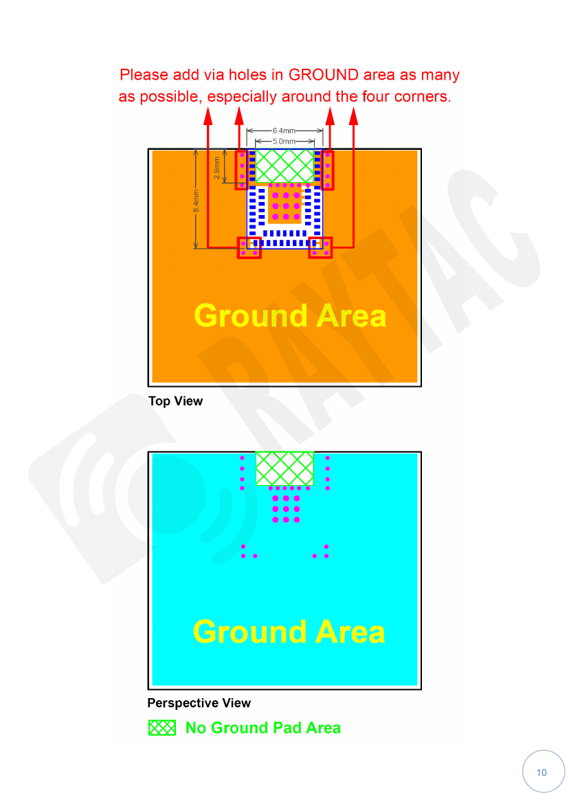
- No Ground-Pad Area: 5.0 × 2.9 mm at the module's antenna end — no copper/ground pads on the host PCB under this zone (all layers). This is nearly identical to the PAN611 keep-out our boards already carry (5.0 × 3.25 mm), so board impact is minimal.
- Antenna GND reference distance ≥ 5 mm on both sides of the module.
- Antenna end toward free space / board edge preferred (performance recommendation).
- Footprint package (land pattern, 2D/3D, reflow profile) is downloaded from Raytac's Support page — do not draw the footprint by hand (DS §2.4).
- Free layout review from Raytac: send design files to sales@raytac.com with subject "Layout Review – Raytac Model No. – CargoBeacon" (DS §2.3).
Measured antenna performance (DS §7, SGS): efficiency 32.0–40.4 % across 2400–2500 MHz (40.4 % @ 2440, 36.0 % @ 2480), peak EIRP +0.57 dBm @ 0 dBm input, reasonably round patterns:
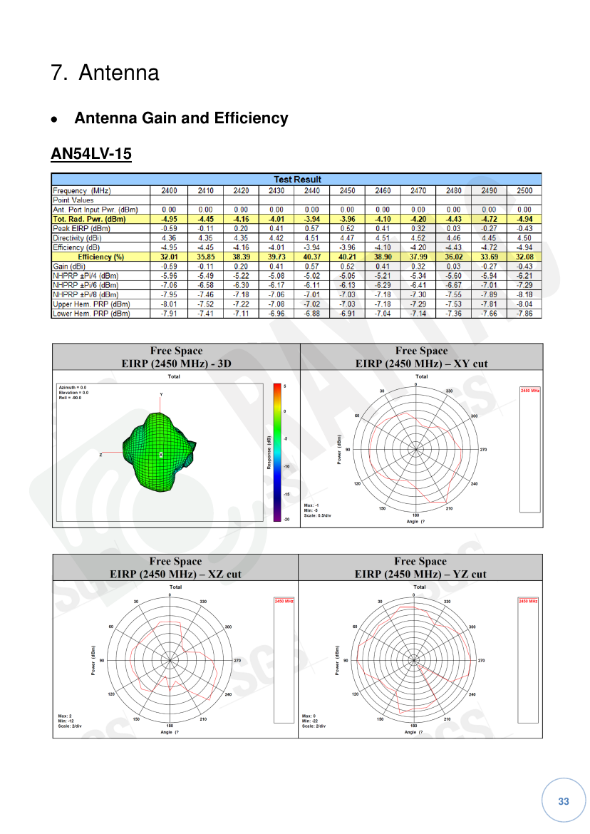
With +8 dBm TX this gives TRP ≈ +4.1 dBm mid-band / +3.6 dBm @ 2480 — on par with the alternatives evaluated in ECN-19, with round patterns.
Host BOM delta vs PAN B611-1¶
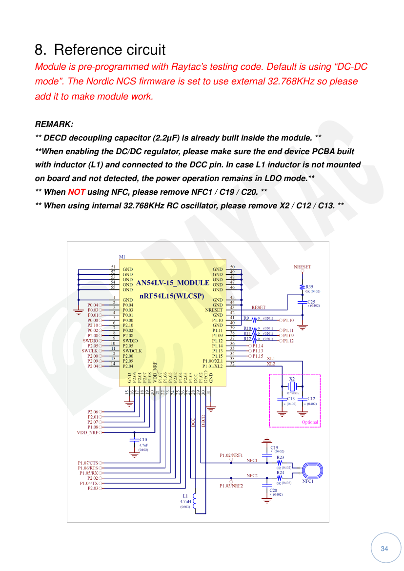
From the reference circuit (DS §8, p. 34):
| Item | Part | Note |
|---|---|---|
| X2 — 32.768 kHz crystal (required for Wirepas) | Epson FC-135R 32.7680KA-AG3 (LCSC C6619114, ~$0.157/1k) — second source Micro Crystal CM8V-T1A-32.768KHZ-7PF-20PPM-TA-QC (DigiKey, $0.263/10k) | CL 7 pF, ±20 ppm, −40…+85 °C — meets Wirepas (±20 ppm @25 °C, −0.04 ppm/°C², ±3 ppm/yr) and nRF54L15 LFXO (CL 6–9 pF, ESR ≤ 100 kΩ). ±10 ppm upgrade option: ECS ECS-.327-7-34B-C-TR9 ($0.339/10k) |
| C12/C13 (crystal load caps) | Omit | nRF54L15 internal load capacitors configured to CL 7 pF (marked "Optional" in DS) |
| L1 — 4.7 µH 0603 between DCC (pad 28) and DECD (pad 30) | Required for DC/DC mode (module default firmware assumption) | Topology per nRF54L15 Datasheet v1.0 §10.3 reference circuit (DCC — L1 4.7 µH 0603 — DECD) and Figure 21. Without L1 the module runs in LDO mode → higher current, and the fallback is silent: DS §5.7.1 — the device probes for an inductor on DCC and stays in LDO if none is detected (VREGMAIN.INDUCTORDET). PAN611 has this internally |
| NFC parts (C19/C20, R23/R24) | Omit | nRF54 internal NFC unused on all boards (ST25DV04K solution unchanged) |
| Decoupling on VDD_NRF | C10 4.7 µF 0402 per DS §8 (p. 34) — corrected 2026-08-23, the page previously said 4.7 nF | DECD 2.2 µF is built into the module |
Certifications¶
| Scheme | ID | Notes |
|---|---|---|
| FCC (US) | SH6AN54LV |
Granted 2025-12-21, C2PC 2026-08-13; covers AN54LV/-K/-P/-U. Label: "Contains FCC ID: SH6AN54LV" (fccid.io) |
| ISED (Canada) | 8017A-AN54LV |
Issued 2025-12-22 (Kiwa); RSS-247/RSS-102. Label: "Contains IC: 8017A-AN54LV" — closes the gap Minew never delivered |
| Bluetooth SIG | Declaration ID Q373526 (QDID Q360916 + Q361608) | BT 6.0 |
| TELEC/MIC (Japan) | 201-250932/00 (2025-12-24) | |
| SRRC (China) | CMIIT 25J71R80V541 (cert 2025-27797, 5 yr) | |
| KC (Korea) | R-R-ryt-AN54LV (2026-01-26) | |
| NCC (Taiwan) | CCAM25Y10270T0 | Per-variant IDs for -P/-U/-K |
| CE RED / UKCA / RCM | SDoC (EN 300 328, EN 301 489-1/-17, EN 55032, IEC 62368-1) | Self-declaration |
Open items¶
- Volume pricing / lead time / supply commitment from Raytac — the remaining commercial gate (order logistics handled outside this documentation)
- Download official footprint package from Raytac Support; Raytac layout review of our placement — first pass received 2026-09-07 (six layout findings → ECN-35, four schematic questions → ECN-36); second pass still open
- EMS X-ray sampling plan for the 55-pad LGA
- Verify DS TX-current figures & sleep currents on eval kit (AN54LV-DB-15)
Related¶
- MCU Modules overview — cross-module pin table
- PAN B611-1 — current module (B1)
- Rev B2 ECN-19 — investigation, decisions, article allocation
- Article Numbering — reserved blocks 232220–239 / 230240–259