Rev B1 ECN-08 — PAN611 stepped footprint (draft)
Draft — EverTag Station only
Replace the U1 (PAN611) module footprint on Connectivity Module PCBs (232200–232204) so solder pads extend outside the component silkscreen outline (stepped-pin style). Not approved. Current revision is A2. Does not apply to Tag (230220) — see Rev B1 ECN-09 — PAN611 stepped footprint.
Ships in the same B1 respin as Rev B1 ECN-01 — GPIO remap. Update the shared Altium footprint cell together with Rev B1 ECN-03 — PAN611 keep-out and Rev B1 ECN-09 — Tag stepped footprint.
Problem (A2)
The physical PAN611 module uses a stepped-pin package, but the U1 footprint in Gerber is drawn as a bottom-soldering type: pads sit fully under the silkscreen / component outline and do not extend outside the body box.
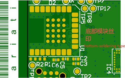
This makes production harder:
- Visual / AOI inspection — no exposed pad edge after placement
- Stencil aperture design — unclear whether apertures may extend beyond the silkscreen box
- Placement QA — operators cannot confirm alignment against visible copper
Proposed fix (B1)
Change U1 to a stepped-pin module footprint: rectangular pads extend outside the silkscreen outline so a strip of copper remains visible, matching good practice elsewhere on the board.
| A2 (current) | B1 (proposed) | |
|---|---|---|
| Footprint style | Bottom-soldering (pads under outline) | Stepped-pin (pads extend outside outline) |
| Pad centres / pitch | Per PAN611 land pattern | Unchanged — geometry exposure only |
| Library | U1 footprint cell | One shared cell — same update as ECN-09 on 230220 |
Scope
| Board | U1 (PAN611) | B1 change |
|---|---|---|
| 232200–232204 | Yes | Update U1 footprint (shared connectivity module layout) |
| 230220 | Yes | ECN-09 — separate Tag doc |
| 232210, 232211 | No | Out of scope |
No BOM or netlist change expected if pad centres and keep-outs remain per PAN B611-1 Product Specification.
Verification before release
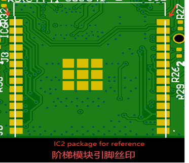
- Land pattern — stepped pad extension matches Panasonic module spec (do not copy IC2 dimensions blindly; IC2 is a layout reference only).
- Antenna keep-out — extended pads on the antenna side must respect corrected keep-out from ECN-03.
- Clearance — check 3D collision with neighbouring passives under U1 (R/C cluster on dense side).
- Stencil — document aperture rules for EMS with exposed pad strips.
- Shared library — one U1 footprint cell; Tag verification on 230220 under ECN-09.
Open items
- Confirm stepped pad dimensions with Panasonic land pattern (or module supplier drawing)
- EMS sign-off on stencil / AOI with stepped U1
- Regenerate Gerber review package after footprint + keep-out updates
Related
- Rev B1 ECN-01 — GPIO remap — same B1 release
- Rev B1 ECN-03 — PAN611 keep-out — same module area
- Rev B1 ECN-09 — Tag PAN611 stepped footprint — 230220
- 232200 Base Std PCB
- PAN B611-1 datasheet — module layout rules
- Revisions Policy — ECN registry