230220 - EverTag Tag Base PCB
| Article Number | 230220 |
| Name | EverTag Tag Base PCB (Wirepas Tag) |
| MCU Module | Panasonic PAN611 (ENW89861B01F, nRF54L15) |
| Key Features | Wirepas tag/anchor, accelerometer, NFC (ST25DV04K), LED, button |
| Power | Battery (V_BAT) |
| Schematic | 230220A1 |
| Status | Active |
1. Overview
The 230220 is the base PCB for the EverTag Tag nRF54 family. It is a compact, battery-powered Wirepas tag/anchor designed for asset tracking and indoor positioning applications. The board carries:
- PAN611 module (ENW89861B01F) -- nRF54L15 MCU with BLE 6.0 and Wirepas Mesh
- LIS2DH12TR accelerometer -- 3-axis MEMS, SPI interface, dual interrupt lines
- ST25DV04K NFC -- external dynamic NFC/RFID tag, I2C interface, external 2-layer coil antenna
- Red LED -- status indication
- Push button (SW1) -- user input
- SWD + UART debug -- via TC2030 tag-connect (P1)
- Board variant detection -- resistor divider on P1.07 ADC (R_bottom = 0 ohm)
- Extension board detection -- reserved ADC on P1.12 (100k pull-down, for future extension boards)
Firmware Compatibility
This board runs the Tag/Anchor (nRF54) firmware build, shared with Station boards 232200 and 232201. The firmware detects this board via the resistor divider on P1.07 (R_bottom = 0 ohm, ADC reads ~0) and initializes the SPI accelerometer, I2C ST25DV NFC, button, and LED accordingly.
Pin-Out Reference Design
230220 is the pin-out reference for all nRF54-based boards. All Station PCBs (232200, 232201, 232202, etc.) must adopt the 230220 pin assignments for shared peripherals. GPIO mux directions are identical across all boards in the Tag/Anchor (nRF54) build group, regardless of whether peripherals are physically populated. See Firmware Compatibility for the GPIO mux master table and variant detection scheme.
Key Differences from Station Base (232200)
| Feature | 230220 (Tag) | 232200 (Station) |
|---|---|---|
| Power | Battery (V_BAT) | 5V from Power Base |
| Voltage regulator | None (direct battery) | TPS62160 buck (5V->3.3V) |
| NFC | ST25DV04K (external, I2C) | ST25DV04K (same, external I2C) |
| Accelerometer | LIS2DH12TR (SPI) | None |
| LED | Red LED (GPIO drive) | WS2812B RGB (single-wire) |
| Button | SW1 (P2.06) | None |
| WiFi expansion | No | Yes (ESP32-C5 on variants) |
2. Block Diagram
graph TB
    subgraph power [Power]
        VBAT["V_BAT"]
    end

    subgraph mcu [BLE Module]
        PAN611["U1: PAN611 - ENW89861B01F"]
    end

    subgraph acc_block [Accelerometer]
        ACC["U3: LIS2DH12TR"]
    end

    subgraph nfc_block [NFC]
        ST25DV["U2: ST25DV04K"]
        ANTENNA["2-Layer Coil Antenna - 11 turns - 7.05x16.5mm"]
    end

    subgraph ui [User Interface]
        LED["D1: Red LED"]
        SW["SW1: Push Button"]
    end

    subgraph debug [Debug / Programming]
        P1["P1: TC2030-CTX-NL"]
    end

    subgraph detect [Board Detection]
        BVAR["B_VARIANT - R6/R7 divider"]
        VSAMP["V_SAMPLE - variant detect"]
    end

    VBAT --> PAN611
    VBAT --> ACC
    VBAT --> ST25DV

    PAN611 -->|"SPI: CLK, SDO, SDI, CS"| ACC
    ACC -->|"INT1, INT2"| PAN611

    PAN611 -->|"I2C: SDA, SCL"| ST25DV
    ST25DV -->|"GPO"| PAN611
    ST25DV -->|"LPD"| PAN611
    PAN611 -->|"VCC enable"| ST25DV
    ST25DV --> ANTENNA

    PAN611 --> LED
    SW --> PAN611

    P1 -->|"SWD + UART"| PAN611

    BVAR --> VSAMP
    VSAMP --> PAN611
Schematic (Sheet 2 of 6 -- BLE, NFC, ACC, Battery)
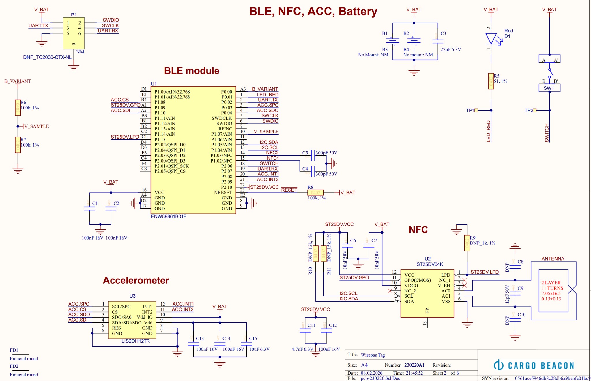
Partial Schematic
The image above shows sheet 2 of 6 from the 230220A1 schematic, covering the BLE module, NFC, accelerometer, and battery sections. Additional sheets (power, connectors, etc.) are maintained in the schematic source files.
3. Pin-Out
3.1 Complete GPIO Assignment
Full pin mapping from the 230220A1 schematic. This is the reference table for firmware development.
| Pin | Name | Pin Type | Function | Connects to | Direction | Notes |
|---|---|---|---|---|---|---|
| 16 | VCC | Power | Power supply | V_BAT | - | Battery voltage |
| 8, 9, 17, A4, D2, E2 | GND | Ground | Ground | GND | - | Multiple ground pads |
| 5 | SWDCLK | Debug | Serial Wire Clock | Debug connector P1 | Input | |
| 6 | SWDIO | Debug | Serial Wire Data | Debug connector P1 | I/O | |
| 23 | nRESET | Reset | Reset input | R8 pull-up (100k, 1%) | Input | Active low, pull-up to V_BAT |
| 7 | RF | RF I/O | RF interface | N/C | - | On-board antenna variant used |
| D1 | P1.00 | Analog | 32.768 kHz crystal | Crystal | - | Used for 32k clock |
| E1 | P1.01 | Analog | 32.768 kHz crystal | Crystal | - | Used for 32k clock |
| A3 | P0.00 | Digital I/O | B_VARIANT | Resistor divider | Input | Board variant detect |
| 1 | P0.01 | Digital I/O | LED_RED | LED D1 via R5 (51 ohm) | Output | Red LED |
| 2 | P0.02 | Digital I/O | UART TX | Debug connector P1 | Output | UART transmit |
| 3 | P0.03 | Digital I/O | ACC.SPC | LIS2DH12TR SCL/SPC (pin 1) | Output | Accelerometer SPI clock |
| 4 | P0.04 | Digital I/O | ACC.SDO | LIS2DH12TR SDO (pin 2) | Input | Accelerometer SPI MISO |
| 10 | P1.07 | Analog | V_SAMPLE | Variant detect resistor | ADC Input | Board variant ID (ADC) |
| 11 | P1.06 | Analog | Board version detect | Not connected | ADC Input | Reserved for PCB revision detect |
| 12 | P1.05 | Digital I/O | I2C SDA | ST25DV04K SDA (pin 5) | I/O | NFC I2C data |
| 13 | P1.04 | Digital I/O | I2C SCL | ST25DV04K SCL (pin 4) | Output | NFC I2C clock |
| 14 | P1.03 / NFC2 | Digital I/O | GPIO reserve | Not connected | - | nRF54 NFC not used on any board; GPIO reserve |
| 15 | P1.02 / NFC1 | Digital I/O | GPIO reserve | Not connected | - | nRF54 NFC not used on any board; GPIO reserve |
| B4 | P1.08 | Digital I/O | ACC.CS | LIS2DH12TR CS (pin 3) | Output | Accelerometer SPI chip select |
| A1 | P1.09 | Digital I/O | ST25DV.GPO | ST25DV04K GPO (pin 1) | Input | NFC general purpose output |
| A2 | P1.10 | Digital I/O | ACC.SDI | LIS2DH12TR SDI/SDA (pin 4) | Output | Accelerometer SPI MOSI |
| B1 | P1.12 | Analog | EXT_DETECT | 100k pull-down to GND | ADC Input | Extension board detection (100k PD) |
| B2 | P1.13 | Analog | Available | - | - | ADC capable, not connected |
| B3 | P1.11 | Analog | Available | - | - | ADC capable, not connected |
| C2 | P1.14 | Analog | Available | - | - | ADC capable, not connected |
| C1 | P1.15 | Digital I/O | ST25DV.LPD | ST25DV04K LPD (pin 7) | Input | NFC low power detect |
| 18 | P2.06 | Digital I/O | SWITCH | Button SW1 | Input | Push button |
| 19 | P2.07 | Digital I/O | UART RX | Debug connector P1 | Input | UART receive |
| 20 | P2.08 | Digital I/O | ACC.INT1 | LIS2DH12TR INT1 (pin 12) | Input | Accelerometer interrupt 1 |
| 21 | P2.09 | Digital I/O | ACC.INT2 | LIS2DH12TR INT2 (pin 11) | Input | Accelerometer interrupt 2 |
| 22 | P2.10 | Digital I/O | ST25DV.VCC | ST25DV04K VCC enable | Output | NFC power enable |
| C4 | P2.00 / QSPI_D3 | Digital I/O | QSPI data 3 | Not connected | - | Available |
| E4 | P2.01 / QSPI_SCK | Digital I/O | QSPI clock | Not connected | - | Available |
| D4 | P2.02 / QSPI_D0 | Digital I/O | QSPI data 0 | Not connected | - | Available |
| E3 | P2.03 / QSPI_D2 | Digital I/O | QSPI data 2 | Not connected | - | Available |
| D3 | P2.04 / QSPI_D1 | Digital I/O | QSPI data 1 | Not connected | - | Available |
| C3 | P2.05 / QSPI_CS | Digital I/O | QSPI chip select | Not connected | - | Available |
Bold rows
Bold rows indicate actively connected signals. Non-bold rows are either power/ground, crystal, or available/unconnected pins.
3.2 Peripheral Summary
| Peripheral | Interface | Pins Used | IC |
|---|---|---|---|
| Accelerometer | SPI | P0.03 (CLK), P0.04 (SDO), P1.10 (SDI), P1.08 (CS) | LIS2DH12TR |
| Accelerometer Interrupts | GPIO | P2.08 (INT1), P2.09 (INT2) | LIS2DH12TR |
| NFC (ST25DV) | I2C | P1.04 (SCL), P1.05 (SDA) | ST25DV04K |
| NFC Control | GPIO | P1.09 (GPO), P1.15 (LPD), P2.10 (VCC enable) | ST25DV04K |
| LED | GPIO | P0.01 (LED_RED) | Red LED D1 |
| Button | GPIO | P2.06 (SWITCH) | SW1 |
| UART | UART | P0.02 (TX), P2.07 (RX) | Debug connector P1 |
| Board Variant | ADC | P1.07 (V_SAMPLE) | Resistor divider R6/R7 (R_bottom = 0 ohm) |
| Extension Detect | ADC | P1.12 (EXT_DETECT) | 100k pull-down to GND |
| Board Version | ADC | P1.06 (reserved) | Not connected |
| SWD | Debug | SWDCLK, SWDIO | Debug connector P1 |
3.3 Debug Connector (P1: TC2030-CTX-NL)
Tag-Connect TC2030-CTX-NL (no-legs variant, 6-pin pogo).
| Pin | Signal | Direction | Notes |
|---|---|---|---|
| 1 | UART.TX (P0.02) | Output | UART transmit |
| 2 | SWDIO | I/O | SWD data |
| 3 | SWDCLK | Input | SWD clock |
| 4 | UART.RX (P2.07) | Input | UART receive |
| 5 | nRESET | Input | Optional reset |
| 6 | GND | - | Ground |
3.4 NFC Antenna
| Parameter | Value |
|---|---|
| Type | 2-layer PCB coil antenna |
| Turns | 11 |
| Dimensions | 7.05 x 16.5 mm |
| Trace width | 0.15 ± 0.15 mm |
| Tuning capacitors | C8, C9, C10 (values per ST25DV04K design guide) |
| Connected to | ST25DV04K AC1/AC0 pins |
3.5 Board Variant Detection
The 230220 uses P1.07 (V_SAMPLE) for base board variant detection via a resistor divider:
| Component | Value | Notes |
|---|---|---|
| R6 (R_top) | 100k 1% | Fixed, connected to VCC |
| R7 (R_bottom) | 0 ohm | Short to GND -- identifies 230220 |
The ADC reads ~0 on this board. Other boards in the same firmware build group (232200, 232201) use different R_bottom values (16.5k steps) to produce distinct ADC readings.
First Prototype Boards
On first prototype boards where R7 may be populated with a non-zero value, unsolder R7 to achieve the expected 0 ohm / GND reading.
Pin P1.12 (EXT_DETECT) is reserved for extension board detection. On 230220, a 100k pull-down resistor connects P1.12 to GND. When no extension board is connected, the ADC reads ~0. An extension board provides its own resistor divider via the board-to-board connector, producing a non-zero ADC reading that identifies the extension variant.
Pin P1.06 is reserved for PCB revision detection (future use).
See Firmware Compatibility for the full detection scheme, ADC windows, and resistor values.
Related Documents
- Firmware Compatibility -- Build matrix, variant detection, GPIO mux master table
- 232200 Station Base Std -- Station base PCB using same MCU module
- Tag nRF54 Family Overview -- Family overview